Internal Wafer Inspection System INSPECTRA® IR Series
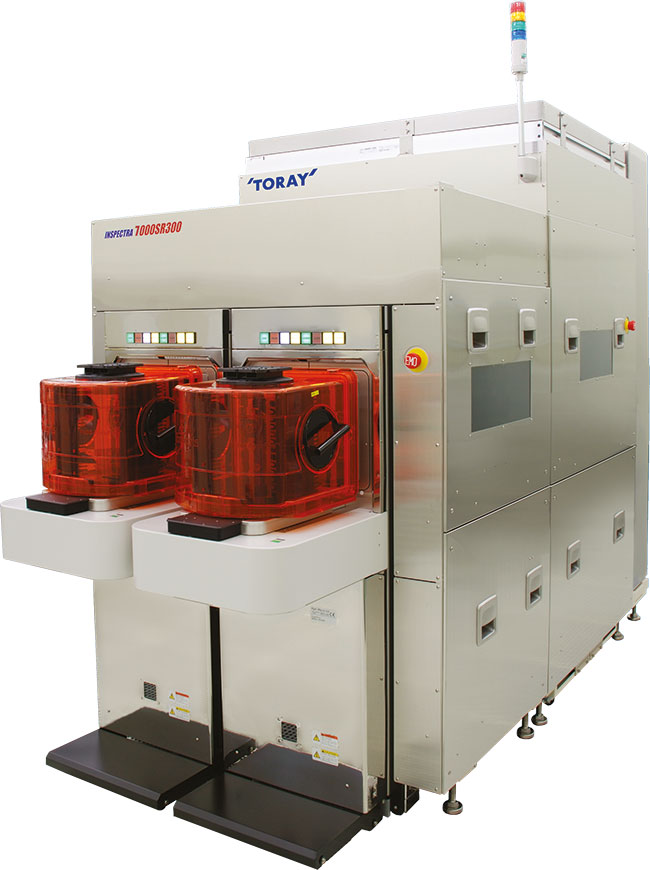
INSPECTRA® 7000 IR 300
Detects defects inside wafers using infrared light
An infrared internal defect inspection system has been added to the INSPECTRA® series. It is now possible to inspect with both infrared and visual light in one system.
Features
- Uses a high-sensitivity camera and newly developed optical system, supporting both infrared and visible light, to rapidly detect internal defects in wafers
- Uses tried and proved quality product learning algorithm to detect minute defects with a high degree of sensitivity
- Inspection can be performed using both infrared and visible light (Switchable)
- Application examples
- Defect inspection in Si capped structure MEMS wafers
- Internal defect inspection in Image Sensor
- Void inspection in bonded wafers
- Defect inspection in high aspect ratio trenches
- Backside crack inspection in High-density wafer
- Pixel resolution

Specifications (IR)
| Pixel resolution | 1µm – |
| Inspection Time | 14 minutes (8 inch wafer, 10x faster) |
| Support Wafer Size | 12 inch & 8 inch and 8 – 2 inches |
Photo Luminescense Defect Inspection System INSPECTRA® PL Series
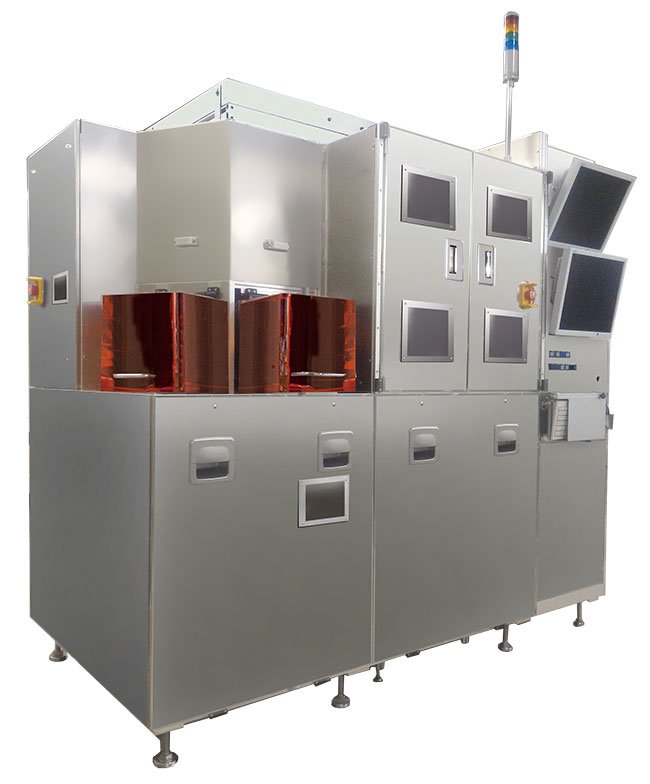
INSPECTRA® PL series
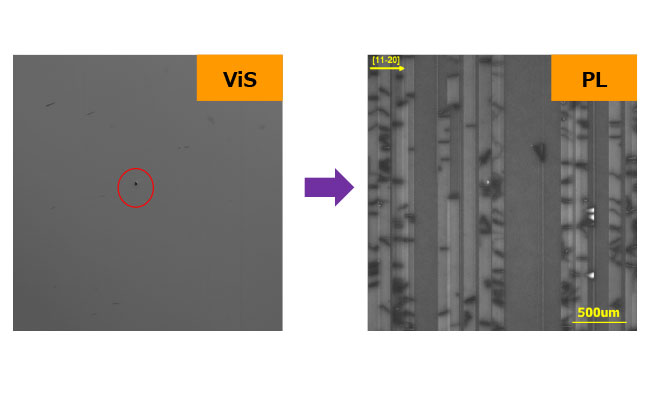
Photo luminescence (PL) is used to automatically inspect for crystal defects, cracks, and luminescence defects which cannot be detected with visible light surface inspection
This system uses luminescent images created using photoluminescence (PL) to perform high-speed, high-sensitivity automatic inspection for crystal defects, cracks, and luminescence defects which cannot be detected with conventional visible light surface inspection!
Features
- Unique optical system and inspection algorithm are used for high-speed, high-sensitivity crystal defect detection and categorization.
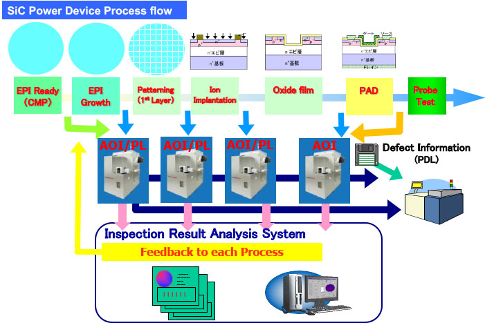
- Can be mounted as an optional peripheral to a wafer inspection system to not only perform crystal defect inspection during EPI processes, but to carry out integrated prototype and mass production inspection that covers everything up to pattern process surface inspection.
- Visible light inspection and PL inspection can be combined to contribute to greater yield by identifying killer defects.
Specifications (PL for GaN, SiC)
| Pixel resolution | 0.65 µm – |
| Inspection Time | 15 minutes (4 inch wafer, 5x faster) |
| Support Wafer Size | 8 – 2 inches |
INSPECTRA® PL series
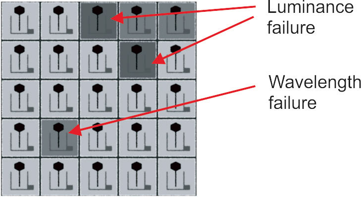
The Pattern Defect and luminescence defect for LED can be inspected.
This system realizes the increase in efficiency of EL TEST.
Features
- This system detects invisible defect of “MQW” and crack.
- Original Optical system and Algorithm.
- Comparing with EL inspection is possible.
Specifications (PL for Micro/Mini LED)
| Inspection Sample | LED wafer, LED chip |
| Pixel resolution | 0.325 µm – |
| Inspection Time | 10 minutes (4 inch wafer, 10x faster) |
| Support Wafer Size | 8 – 2 inches |
| Inspection Functions | PL and AOI |
